In the realm of modern electronics, Printed Circuit Boards (PCBs) stand as the backbone of nearly all electronic devices, from smartphones to complex medical equipment and spacecraft. The process of PCB manufacturing has evolved significantly over the years, driven by technological advancements and the ever-increasing demands for smaller, faster, and more efficient electronic devices. In this article, we delve into the intricacies of PCB manufacturing, exploring its key stages, innovations, challenges, and the future prospects of this vital industry.
Understanding PCB Manufacturing
At its core, PCB manufacturing involves the creation of a substrate or base material onto which electronic components are mounted and interconnected to create functional circuits. The process typically involves several key stages:
Design and Prototyping:
Engineers create a schematic of the circuit layout using specialized software. This design is then translated into a prototype PCB, often through techniques like computer-aided design (CAD) and rapid prototyping technologies.
1.Substrate Preparation:
The base material for PCBs is typically made of fiberglass-reinforced epoxy laminate known as FR-4. Copper foils are laminated onto these substrates, forming the conductive layers of the PCB.
2.Etching:
A chemical etching process removes excess copper from the substrate, leaving behind the desired circuit pattern. Advanced techniques such as laser etching have also gained prominence for high-precision applications.
3.Drilling:
Holes are drilled into the PCB to accommodate component leads and interconnect layers.
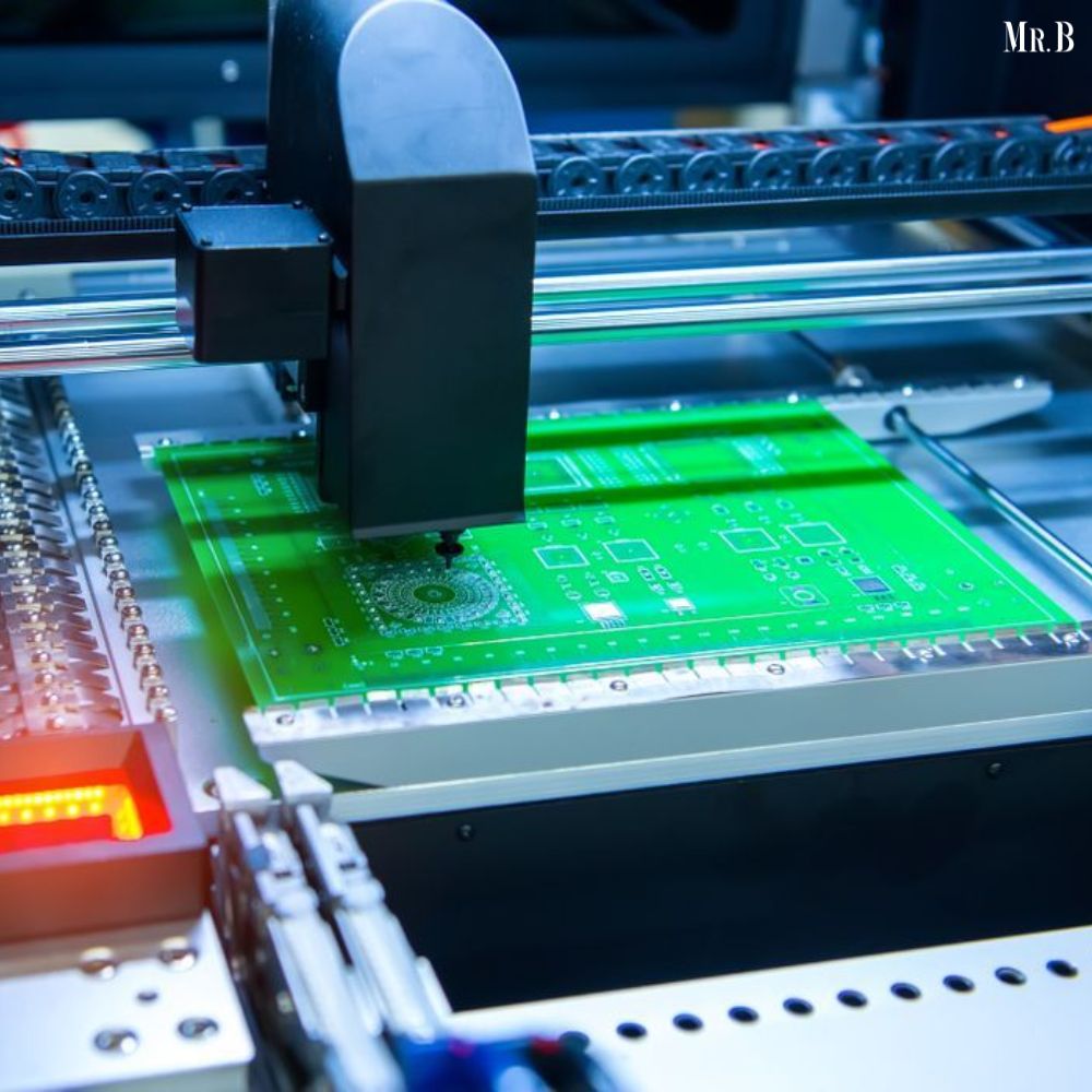
4.Component Placement:
Automated pick-and-place machines precisely position electronic components onto the PCB according to the design specifications.
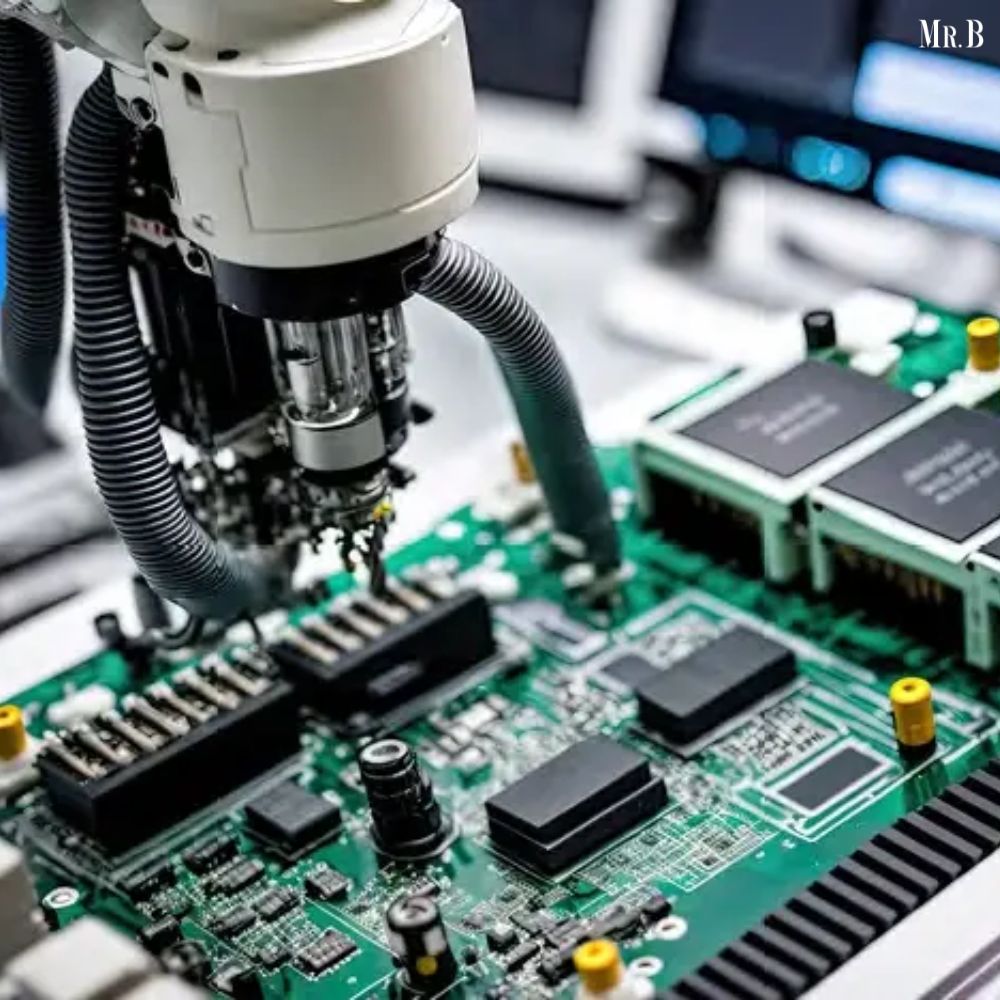
5.Soldering:
Components are soldered onto the PCB to establish electrical connections. Surface Mount Technology (SMT) and Through-Hole Technology (THT) are two common soldering methods used in PCB assembly.
6.Testing and Quality Control:
Finished PCBs undergo rigorous testing to ensure functionality, reliability, and adherence to industry standards such as IPC-A-600 for quality acceptance criteria.
Innovations Driving PCB Manufacturing
1. Miniaturization and High-Density Interconnects
One of the most notable trends in PCB manufacturing is the relentless drive towards miniaturization and higher component densities. This trend is fueled by consumer demands for sleeker devices with increased functionality. Advanced manufacturing techniques such as multilayer PCBs, Microvias, and HDI (High-Density Interconnect) technology enable designers to pack more functionality into smaller form factors while maintaining signal integrity and thermal management.
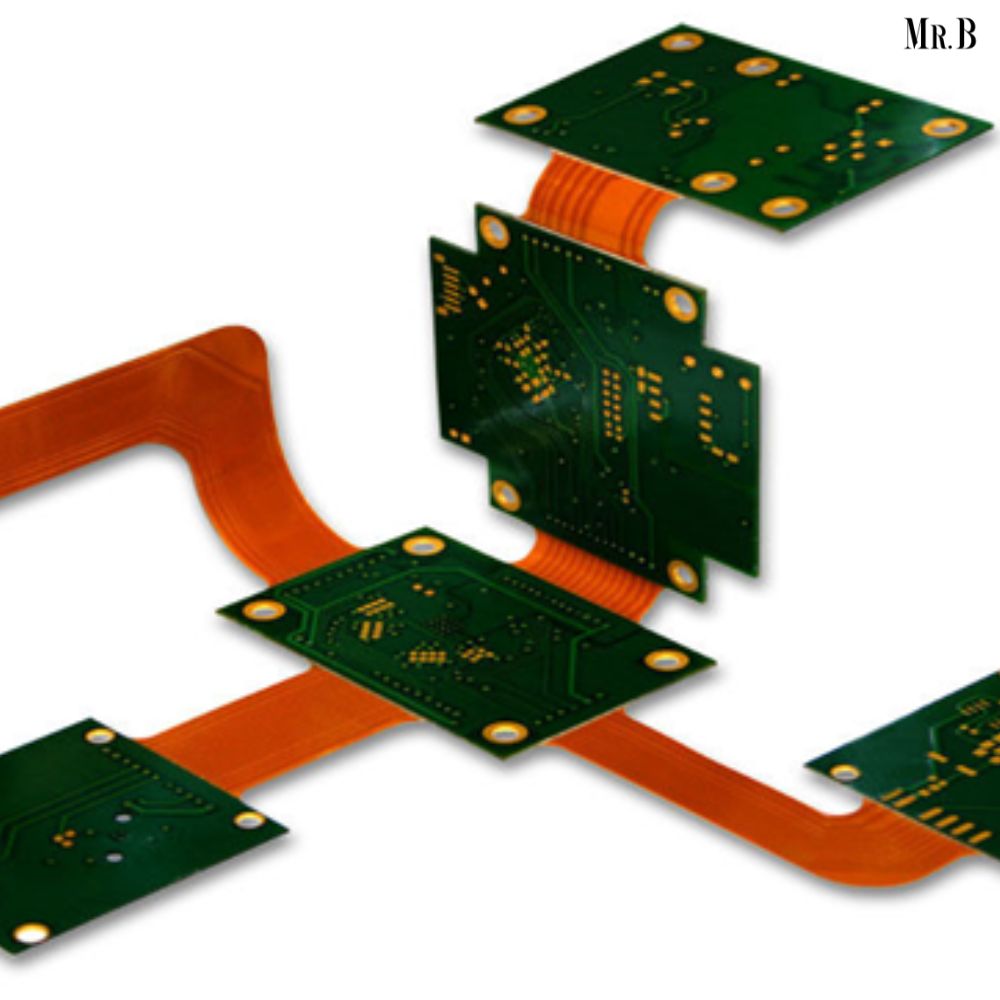
2. Flexible and Rigid-Flex PCBs
Traditional rigid PCBs are giving way to flexible and rigid-flex PCBs in applications where flexibility, space constraints, or dynamic movement are critical factors. Flexible PCBs, made from polyimide or polyester substrates, offer bendability and can be shaped to fit into unconventional spaces. Rigid-flex PCBs combine rigid and flexible substrates, offering versatility in design and durability in harsh environments.
3. Advanced Materials and Finishes
The choice of materials and surface finishes significantly impacts PCB performance, reliability, and manufacturability. Innovations in materials such as high-frequency laminates, ceramic-filled PTFE (Polytetrafluoroethylene), and metal core substrates cater to specific application needs such as high-speed data transfer, thermal management, and harsh environment resistance. Surface finishes like ENIG (Electroless Nickel Immersion Gold) and OSP (Organic Solderability Preservatives) enhance solderability and corrosion resistance.
4. Automation and Industry 4.0 Integration
Automation plays a pivotal role in streamlining PCB manufacturing processes, reducing human errors, and enhancing productivity. Advanced robotics, AI-driven quality control systems, and machine learning algorithms are integrated into manufacturing lines, enabling real-time monitoring, predictive maintenance, and adaptive manufacturing processes. Industry 4.0 principles such as IoT (Internet of Things) connectivity, digital twins, and smart factories are reshaping the PCB manufacturing landscape, fostering agility and competitiveness.
5. Environmental Sustainability
Sustainable practices are gaining traction in PCB manufacturing to minimize environmental impact and comply with regulatory standards. Initiatives such as lead-free soldering, recycling of electronic waste (e-waste), and eco-friendly substrate materials contribute to a greener and more responsible electronics industry. Manufacturers are also adopting energy-efficient processes and optimizing resource utilization throughout the PCB lifecycle.
Challenges and Future Trends
While PCB manufacturing has witnessed remarkable advancements, several challenges persist, shaping future trends and innovations in the industry:
1.Complexity vs. Reliability:
As PCB designs become more complex with miniaturization and high-speed requirements, ensuring reliability in terms of signal integrity, thermal management, and electromagnetic compatibility (EMC) remains a paramount challenge. Advanced simulation tools, material selection expertise, and robust testing methodologies are crucial in addressing these reliability concerns.
2.Supply Chain Disruptions:

Global supply chain disruptions, as seen during the COVID-19 pandemic, highlight the vulnerabilities inherent in the electronics manufacturing ecosystem. Diversification of suppliers, localized production capabilities, and resilient logistics strategies are essential for mitigating supply chain risks and ensuring continuity.
3.Cybersecurity Concerns:
With the proliferation of connected devices and IoT-enabled systems, cybersecurity threats pose significant risks to PCBs and electronic systems. Secure design practices, encryption protocols, and hardware-level security features are integral to safeguarding against cyberattacks and data breaches.
4.Materials Innovation:
Advancements in materials science, including nanomaterials, conductive inks, and flexible substrates, are poised to revolutionize PCB manufacturing. Materials with enhanced thermal conductivity, mechanical flexibility, and environmental sustainability will drive future PCB designs for emerging technologies such as 5G, IoT, and electric vehicles (EVs).
5.AI and Data Analytics:
The integration of artificial intelligence (AI) and data analytics in PCB manufacturing processes offers insights into production efficiencies, defect detection, and predictive maintenance. AI-driven algorithms optimize manufacturing parameters, identify anomalies, and improve overall quality control, paving the way for smarter and more adaptive manufacturing systems.
Emerging Technologies Shaping PCB Manufacturing
As we look ahead, several emerging technologies hold the potential to reshape PCB manufacturing processes and capabilities:
1. 5G and IoT Integration
The widespread deployment of 5G networks and the proliferation of IoT devices are driving demand for PCBs optimized for high-speed data transfer, low latency, and connectivity scalability. PCB designs tailored for RF (Radio Frequency) performance, antenna integration, and signal integrity are critical for next-generation wireless communications and IoT ecosystems.
2. AI-Driven Design and Manufacturing
Artificial intelligence (AI) and machine learning (ML) are revolutionizing PCB design, optimization, and manufacturing. AI-driven design tools assist engineers in layout optimization, signal routing, and thermal analysis, leading to enhanced performance, reduced design iterations, and faster time-to-market. In manufacturing, AI-powered quality control systems detect defects, optimize process parameters, and predict maintenance requirements, ensuring higher yields and product reliability.
3. Embedded Systems and Edge Computing
The convergence of embedded systems and edge computing requires PCBs with integrated functionalities, compact footprints, and efficient power management. Advanced PCB technologies such as System-on-Chip (SoC) integration, stacked dies, and embedded sensors enable seamless integration of computing power, connectivity, and real-time data processing at the network edge, supporting applications in autonomous vehicles, industrial automation, and smart infrastructure.
4. Advanced Packaging Solutions
Innovations in packaging technologies play a crucial role in enhancing PCB performance, reliability, and miniaturization. Three-dimensional (3D) packaging, System-in-Package (SiP), and Chip-on-Board (CoB) architectures enable compact designs, reduced interconnect lengths, and improved thermal dissipation, addressing challenges posed by high-density components and heterogeneous integration in modern electronic systems.
5. Green Manufacturing and Circular Economy
The electronics industry is increasingly embracing green manufacturing practices and adopting circular economy principles to minimize waste, energy consumption, and environmental impact throughout the PCB lifecycle. From eco-friendly materials and lead-free processes to efficient recycling and end-of-life management, sustainable initiatives drive innovation, compliance with regulations, and positive environmental stewardship within the PCB manufacturing ecosystem.
Collaborative Ecosystem and Future Prospects
The future of PCB manufacturing hinges on collaborative partnerships across industry sectors, academia, and research institutions. Key areas of focus and opportunities for innovation include:
1.Materials Advancements:
Research and development in novel materials such as graphene-based substrates, conductive polymers, and biodegradable composites offer breakthrough possibilities in performance, sustainability, and cost-effectiveness for next-generation PCBs.
2.Digital Twins and Virtual Prototyping:
Digital twins and virtual prototyping simulations enable comprehensive analysis, optimization, and validation of PCB designs and manufacturing processes in virtual environments, reducing time-to-market and enhancing product quality.
3.Supply Chain Resilience:
Building resilient supply chains through digitalization, predictive analytics, and strategic partnerships ensures continuity, agility, and risk mitigation against global disruptions and market fluctuations.
4.Cyber-Physical Systems Security:
Integration of robust cybersecurity measures, hardware authentication, and secure communication protocols strengthens the resilience of PCBs and electronic systems against cyber threats, data breaches, and tampering.
5.Industry Standards and Regulatory Compliance:
Adherence to international standards such as IPC (Association Connecting Electronics Industries) guidelines, RoHS (Restriction of Hazardous Substances) directives, and emerging regulatory frameworks fosters interoperability, quality assurance, and responsible manufacturing practices across the PCB industry.
Conclusion: Navigating Towards Technological Excellence
In conclusion, the landscape of PCB manufacturing is characterized by rapid technological advancements, evolving market demands, and sustainability imperatives. Innovations spanning materials science, automation, connectivity, and environmental stewardship are driving the industry towards greater efficiency, reliability, and adaptability in a digitally interconnected world.
Collaborative ecosystems, interdisciplinary research endeavors, and a commitment to ethical, sustainable practices are essential pillars shaping the future trajectory of PCB manufacturing. By embracing emerging technologies, fostering innovation ecosystems, and addressing global challenges collaboratively, the industry is poised to navigate complexities, seize opportunities, and lead the way towards technological excellence in the dynamic realm of modern electronics.
Curious to learn more? Explore this Article on: Mr. Business Magazine